- All
- Product Name
- Product Keyword
- Product Model
- Product Summary
- Product Description
- Multi Field Search
Views: 0 Author: Site Editor Publish Time: 2026-08-28 Origin: Site
IGBT Snubber Capacitors are selected to control the voltage overshoot and ringing that appear when an IGBT commutates current in a real, inductive power loop. The task is not simply to choose the largest capacitance or the highest voltage rating. A good selection starts with the measured switching waveform, the available voltage margin of the IGBT, the loop inductance, and the energy that must be absorbed repeatedly. This guide focuses on the practical choices that affect protection in inverter stages, motor drives, UPS systems, renewable-energy converters, and other high-power switching equipment.
Start with the actual turn-off waveform and the IGBT’s allowed voltage margin; nominal DC-link voltage alone is not enough.
Select capacitance together with ESR, ESL, pulse-current capability, voltage rating, temperature, and the physical connection method.
Treat the capacitor, resistor, busbar, and mounting loop as one snubber system rather than independent parts.
A low ESL capacitor mounted directly in the commutation loop can be more effective than a larger part installed remotely.
Validate the final RC snubber circuit at operating current, temperature, and switching frequency before releasing the design.
An IGBT can switch current quickly, but current flowing through stray inductance cannot stop instantly. When the IGBT turns off, the changing current produces an additional voltage across the inductive path. A useful first-order relationship is:
V_overshoot ≈ L_stray × di/dt
The measured peak at the IGBT is influenced by more than this simple equation. Device behavior, diode recovery, busbar geometry, probe method, and the resonant network all matter. Still, it explains why a compact high-current assembly can develop harmful overshoot even when the DC-link voltage seems comfortably below the IGBT blocking rating.
An IGBT snubber capacitor provides a nearby path for transient current. It slows the voltage rise, shares part of the transient energy, and can reduce the amplitude of ringing. In an RC network, the resistor dissipates energy and damps the capacitor–inductance resonance. In an RCD arrangement, the diode can steer current so the network acts primarily during the intended part of the switching event. The appropriate topology depends on the converter, the switching device, and the loss budget; a capacitor cannot be specified correctly until that function is clear.
For a concise overview of the circuit families and their uses, see this guide to snubber capacitor types. In every topology, the selection objective is the same: keep the semiconductor within its permitted voltage and current stress while avoiding excessive heat or unnecessary switching loss in the snubber itself.
The first design question is not “What capacitance should I use?” It is “What event must the network control?” In an inverter leg, the critical event is often IGBT turn-off at the worst credible current and DC-link condition. In other converters, transformer leakage inductance, a diode recovery event, or a cable-induced resonance may be dominant. Measure the waveform at the device terminals with a probing arrangement that does not add a long ground lead or create a misleading ringing frequency.
Record the DC-link voltage, peak collector current, peak collector-emitter voltage, ringing frequency, switching frequency, heat-sink and local ambient temperatures, and the operating state that produced the waveform. Fault and overload cases deserve separate attention. A snubber that looks adequate at normal load may provide little margin when current rises quickly during a transient condition.
The voltage target should include an engineering margin below the IGBT’s repetitive or transient limit, as applicable to the device data sheet and operating conditions. Avoid translating a generic voltage ratio directly into a component rating. The capacitor sees its own combination of DC bias, transient peak, AC ripple, and temperature. The resistor and diode, where used, also see pulse conditions that must be checked independently.
Capacitance affects both suppression and resonant behavior. If the local loop inductance is approximately known, the undamped resonant frequency can be estimated as:
f0 ≈ 1 / (2π√(L_stray × C_snub))
This estimate is useful for comparing candidate values, not for replacing waveform tests. Larger capacitance can take more energy for a given voltage rise, but it can also increase turn-on current, resistor dissipation, package volume, and the severity of an inadequately damped discharge. The best IGBT snubber capacitor is therefore the one that meets the measured protection target with acceptable losses and layout, not necessarily the largest available value.
Use a candidate data sheet only after the switching event and network topology are defined. The table below connects each selection input to the check that prevents a common design mistake.
Parameter | What to Check |
Voltage rating | Maximum measured voltage + required margin |
Capacitance | Required to limit voltage overshoot |
ESR | Switching loss and capacitor heating |
ESL | Voltage spike caused by internal and mounting inductance |
Pulse current | Peak and repetitive switching current |
dv/dt | Maximum voltage rise rate |
Temperature | Hot-spot temperature and lifetime |
Package | Short, low-inductance connection to the IGBT |
Voltage selection begins with the true waveform, then includes DC bias and temperature. A capacitor may withstand a short peak but still require derating for continuous voltage or elevated temperature. Read the manufacturer’s rating definitions carefully: DC rating, AC rating, pulse voltage, and test voltage are not interchangeable.
For pulse energy, a useful bounding calculation is the change in stored energy when a capacitor moves from an initial voltage to a peak voltage:
ΔE = ½ × C × (V_peak² − V_initial²)
This is only one part of the design calculation. The actual current waveform, circuit topology, and resistor path determine where that energy goes and how often the capacitor experiences it. Use the measured oscillatory current or a verified simulation to compare against the capacitor’s pulse-current capability. A pulse current capacitor should be evaluated for repeated stress over the duty cycle, not judged from a single clean pulse.
For many high-power IGBT applications, a polypropylene film capacitor is a practical choice because film constructions can offer low loss, high pulse capability, and stable behavior for repetitive switching duty. It is still important to select the particular construction rather than treating “film” as a complete specification. Electrode design, winding geometry, terminals, encapsulation, and heat removal all influence the usable limits.
Low ESR reduces resistive loss, while a low ESL capacitor reduces the voltage developed inside the component and connecting loop during fast current transitions. These terms should be evaluated together. A compact component with suitable internal construction can lose its advantage if it is connected through long, narrow conductors. Conversely, a mechanically convenient remote location may be electrically ineffective because the IGBT remains separated from the snubber by the very inductance causing the overshoot.
Terminations are a design choice, not a packaging afterthought. Wide lugs or busbar-friendly terminals can help create a broad, short current path at high current. Axial leads can suit layouts where the loop is naturally compact, but their inductance and lead geometry must be included in the evaluation. Clearance, creepage, vibration, fastening torque, and insulating barriers must be reviewed alongside electrical performance.
The IGBT/GTO snubber capacitor portfolio is intended for power-electronics switching protection and describes the value of low ESR and low ESL in that role. For a product-level starting point, the SMJ-P IGBT snubber capacitor lists its voltage and capacitance ranges, but the final choice still requires checking the complete data sheet against the measured application waveform.
CRE offers several IGBT/GTO snubber capacitor configurations for different switching and installation requirements.
SMJ-P: Plastic-box construction for compact IGBT protection and flexible mounting.
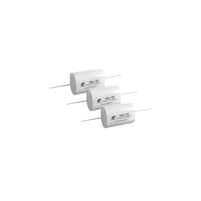
SMJ-TE: Axial-lead construction for applications requiring a compact axial connection.
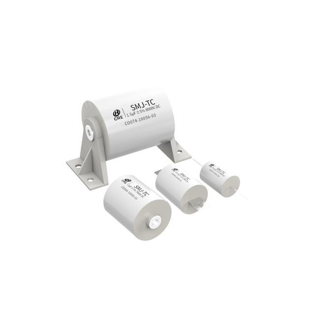
SMJ-TC: High-voltage GTO snubber applications with high pulse and dv/dt requirements.
All three should be evaluated against the actual switching waveform, voltage, pulse current, temperature, and available installation space.
CRE also provides custom snubber capacitor solutions for specific capacitance, voltage, dimensions, terminal configuration, and mounting requirements. For a custom recommendation, engineers can provide the DC-link voltage, switching frequency, peak current, measured overshoot, and installation constraints.
In a simple capacitor-only network, transient energy can move back and forth between the capacitor and stray inductance. That behavior can replace one peak with a sustained ring. An RC snubber circuit adds a resistor so energy is dissipated and the resonance is damped. An RCD network adds directionality and can be useful when it is important to limit loss or control the capacitor’s charge and discharge path.
An initial resistor estimate is sometimes based on the characteristic impedance of the local resonant path:
R_start ≈ √(L_stray / C_snub)
Use this as a test value, not a final answer. The effective resistance in a real converter includes semiconductor behavior, the capacitor’s ESR, wiring, and any nonlinear elements. Change the resistance around the starting point while observing peak voltage, ringing, peak current, average resistor dissipation, and turn-on behavior. The best damping point balances those outcomes rather than minimizing only one peak on one oscilloscope capture.
The resistor needs suitable pulse-energy capability, voltage withstand, temperature performance, and low enough parasitic inductance for its position in the loop. The diode in an RCD circuit must be reviewed for reverse voltage, surge current, recovery behavior, and thermal stress. These checks matter because moving loss out of the IGBT does not eliminate it; the loss must be managed somewhere in the snubber network.
Placement is often the difference between a successful selection and a disappointing result. The snubber must bridge the section of the commutation path that produces the troublesome inductive voltage. Putting it near the power stage but outside that critical loop can leave the IGBT exposed. Keep the outgoing and return conductors close together, use short and broad connections where possible, and avoid remote leads that enlarge the loop area.
On a PCB, this may mean using adjacent planes or overlapping copper paths. In a laminated-busbar design, it may mean fastening the capacitor directly across the relevant module terminals or busbar nodes. The exact geometry is application-specific, but the question is consistent: at the instant of turn-off, can the transient current reach the capacitor without first passing through a long inductive path?
This IGBT snubber capacitor placement guidance is a useful companion to the electrical selection because it focuses on the commutation loop rather than the nearest available mounting space. Include the final connection geometry in design reviews and production drawings; a component substitution or an extra lead length can alter the result materially.
Prototype validation should reproduce the conditions that matter to the finished equipment. Check start-up, normal-load switching, overload or fault behavior where safe and permitted, maximum DC-link voltage, high and low temperature, and the intended switching-frequency range. Inspect both turn-off and turn-on waveforms. A snubber that reduces turn-off overshoot may add capacitor-discharge current during the next transition, so neither event should be evaluated in isolation.
Verify the measurement method before making close margin decisions. A probe loop that is much larger than the power loop can show ringing that the device does not actually see, while a poor reference point can hide a local peak. Correlate oscilloscope results with thermal measurements of the capacitor, resistor, and nearby conductors after the system reaches steady state.
Then repeat the test with production-representative parts. Capacitance tolerance, busbar alignment, fastener quality, and position changes can shift resonant behavior. Document the allowed component, its mounting orientation, conductor dimensions, torque requirements, and acceptable waveform limits. That turns a successful lab adjustment into reliable inverter IGBT protection rather than an undocumented one-off result.
Ask for the data that supports the specific duty: voltage and temperature limits, capacitance tolerance, ESR or dissipation factor, ESL or construction information, permitted RMS current, pulse-current and dv/dt limits, terminal configuration, and thermal conditions for the stated ratings. If the converter has an unusual waveform, share the measured traces and operating envelope with the supplier rather than matching parts by capacitance alone.
A supplier discussion around capacitance, voltage rating, and package requirements is most productive when it includes the circuit topology, DC-link range, switching frequency, measured overshoot, peak current, available installation space, and a drawing or photograph of the commutation path. Those inputs allow a candidate to be assessed as part of the real assembly.
Selecting IGBT Snubber Capacitors is a system-level exercise. Begin with the turn-off event and the permissible IGBT voltage, estimate the role of local inductance, then choose capacitance, voltage capability, ESR, ESL, pulse endurance, and termination as a coordinated set. Add damping deliberately, place the network inside the critical current loop, and confirm the result with properly captured electrical and thermal measurements. With that approach, CRE NEW ENERGY PTE. LTD. and the design team can evaluate a suitable snubber solution against real converter stress instead of relying on a nominal capacitor value alone.
Select it based on measured voltage overshoot, IGBT voltage margin, capacitance, ESR, ESL, pulse current, dv/dt, temperature, and mounting inductance. Do not select the capacitor by DC-link voltage or capacitance alone.
There is no universal value. The required capacitance depends on stray inductance, switching current, voltage overshoot, switching frequency, and the target damping performance. Candidate values should be validated on the actual converter.
Yes. CRE can customize capacitance, voltage rating, dimensions, terminal configuration, and mounting requirements for IGBT and GTO switching applications.